74HC165 sense-chain reference
Three cascaded 74HC165 shift registers read up to 24 matrix sense lines through three Pico
GPIO. This page is the electrical reference; the firmware side is in
../firmware/architecture.md.
Datasheet: Nexperia 74HC_HCT165.
How a 74HC165 works
PLLOW → the eight inputs D0–D7 are loaded into the register asynchronously.PLHIGH → each rising edge onCPshifts the register one bit towardQ7, pulling a new bit in fromDS.CEmust be LOW forCPto do anything.Q7is the serial output;DSis the serial input from the previous device in a chain.
So one read is: pulse PL low, then clock 8 × n bits out while reading Q7.
Chain schematic
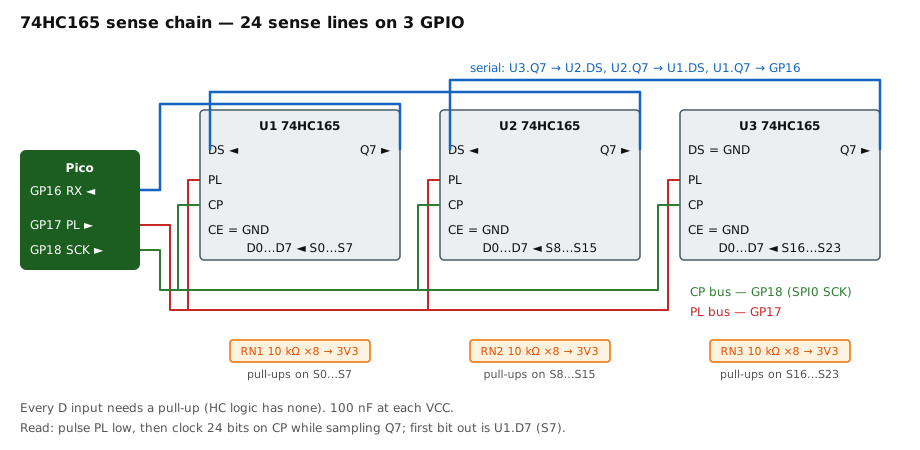
                 Pico
   GP17 (PL)  ───┬─────────────────┬─────────────────┐
   GP18 (CP)  ──┬┼────────────────┬┼────────────────┐│
                ││                ││                ││
            ┌───┴┴────┐       ┌───┴┴────┐       ┌───┴┴────┐
            │ U1      │       │ U2      │       │ U3      │
   GP16 ◄───┤Q7     DS│◄──────┤Q7     DS│◄──────┤Q7     DS│◄── GND
            │ 74HC165 │       │ 74HC165 │       │ 74HC165 │
            │CE=GND   │       │CE=GND   │       │CE=GND   │
            │D0..D7   │       │D0..D7   │       │D0..D7   │
            └─┬┬┬┬┬┬┬┬┘       └─┬┬┬┬┬┬┬┬┘       └─┬┬┬┬┬┬┬┬┘
              S0 … S7           S8 … S15          S16 … S23      ← sense lines from FPC
              ││││││││          ││││││││          ││││││││
             [RN1 10k×8]       [RN2 10k×8]       [RN3 10k×8]     ← bussed SIP pull-ups
                 │                  │                  │
                3V3                3V3                3V3
Bit order on the wire: the first bit clocked out of GP16 is U1’s D7 (S7), the last
is U3’s D0 (S16). Document the mapping once in firmware and never reason about it twice.
Wiring rules
| Pin | Connection | Why |
|---|---|---|
VCC |
3V3, with 100 nF to GND at each chip | HC logic, 2.0–6.0 V range |
CE |
GND on every device | clock enable must be LOW or nothing shifts |
DS of U3 (last) |
GND | defines the bits that shift in past the end of the chain |
D0–D7 |
sense line and 10 kΩ pull-up to 3V3 | no internal pull-ups — floating inputs read random keys |
PL |
all three in parallel to GP17 | one latch pulse loads all 24 bits at once |
CP |
all three in parallel to GP18 | |
Q7 |
U3 → U2 DS, U2 → U1 DS, U1 → GP16 |
Use 9-pin bussed SIP networks (common pin to 3V3) — three parts instead of twenty-four resistors on a stripboard. On the Rev B PCB these become 4 × 0603 arrays.
Scan sequence
for each drive line Dk in GP0..GP9:
    set Dk LOW                        (others high-Z / high)
    wait MATRIX_IO_DELAY              (~30 µs; lets the pull-ups settle)
    PL LOW for ≥ 100 ns, then HIGH    (latch all 24 sense inputs)
    clock 24 bits over SPI0, MSB first, reading GP16
    release Dk
    row[k] = ~bits & mask             (a pressed key reads LOW)
Timing from the datasheet at 3.3 V is generous: PL pulse width min ~25 ns, CP up to
~30 MHz. SPI0 at 8 MHz has ~4× margin. Full scan ≈ 350 µs for 10 drive lines.
Failure modes and what they look like
| Symptom | Cause |
|---|---|
| Random keys with nothing pressed | A sense input is floating — missing pull-up, or the SIP network’s common pin is not on 3V3 |
| Every key reads as the same column, or a stuck pattern | PL and CP swapped, or CE left floating |
| Keys appear shifted by 8 | Chain order assumption wrong — U1/U3 Q7 → DS crossed |
| Whole chain dead | CE not grounded, or DS of the last device floating and reading as bits |
| Keys work but ghost with three held | Not a chain problem — the membrane lacks diodes. See Phase 1 |
The tools/shift_register_test/ CircuitPython script (M2) exercises the
chain with nothing else connected: ground each sense input in turn and watch the bit
position light up.
Why not the 74HC595
The 595 is the output counterpart (serial-in, parallel-out). It would expand the drive side instead. We have 10 spare drive GPIO and the chain only needs to expand sensing, so a 165 is the right part. If probing finds a transposed matrix, the chain moves to whichever side is larger — still 165s, still sensing.